Selective growth for the integration of an amplitude modulator and a waveguide
:: References :: Other projects
Selective growth consists in growing epitaxial layers on a patterned substrate. Different regions of the substrate are exposed to growth and others are covered with a dielectric. Growth occurs only on the exposed region. The growth rate and the alloy composition of the grown material depends on the geometry of both the exposed and covered areas. Therefore, the width and the alloy composition of a selective grown quantum well depends on the pattern geometry. Consequently, it is possible to have on the same growth and same substrate regions with different optical transition energies. It is then possible to integrate a waveguide or light source with a modulator.
InGaAs/InAlAs quantum wells were grown on patterned substrates to study the optoelectronic integration of a modulator with a waveguide. First, both the growth rate enhancement and the alloy composition were calibrated for InGaAs and InAlAs measuring X-ray diffraction and low temperature photoluminescence on a satellite sample gorwn on an unprocessed substrate. The rdata were compared with results from atomic force microscopy, photoluminescence and spatial perfilometry on the samples grown on the patterned substrates. It is well-known that for the growth of bulk In containing alloys on unpatterned substrates, the In source flux, TMIn, should be higher than that of the Ga (TMGa) or Al (TMAl) sources if layers with the same In and Ga or Al content are desired. On the other hand, in the window of masked substrates both the InGaAs and InAlAs are In rich compared to the same material grown on the unmasked substrates for the same growth input parameters. A substantial decrease of fluxes ratio of TMIn with respect to TMGa or TMAl was found as a function of the mask width for obtaining InGaAs and InAlAs layers lattice matched to InP.
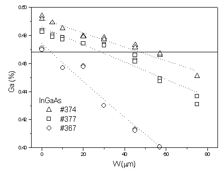
Fig. 1 Ga content of the InGaAs alloy for samples grown with different [TMIn / (TMIn + TMGa)] fraction in the gas phase as a function of mask width (W). The dotted lines are exponential decay fits. The horizontal line refers to lattice matched InGaAs grown on InP substrates.
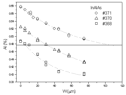
Fig. 2 Al content of the InAlAs alloy for samples grown with different [TMIn / (TMIn + TMGa)] fraction in the gas phase as a function of mask width (W). The dotted lines are exponential decay fits. The horizontal line refers to lattice matched InAlAs grown on InP substrates.
MQW structures to be used in the fabrication of modulators to operate at 1.55 µm should have a precise lowest optical transition energy. This energy depends on both the growth enhancement and the alloy composition. Photoluminescence and stylus profiler results together with a calculation of the Schrödinger equation within the effective mass approximation, allowed one to determine the In content of the alloy in the QWs as a function of the mask width for different flux ratios of the elements III. The In content of the alloy increases exponentially with the mask width for all studied samples, saturating for masks larger than 40 to 50 µm. Thus, two regimes can be distinguished. For masks smaller than 40 µm both growth enhancement and changes in alloy composition determine the optical transition energy while, for masks larger than 50 µm, the alloy composition remains stable and the selectivity is essentially due to the growth enhancement.
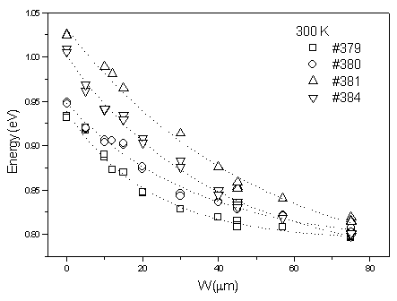
Fig. 3 Lowest optical transition energy for a series of InGaAs/InAlAs MQW structures grown with various [TMIn / (TMIn + TMGa)] fraction in the gas phase and growth times as a function of mask width (W). The dotted lines are exponential decay fits.
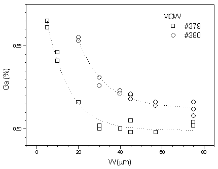
Fig. 4 Ga content in the InGaAs QW alloy for two InGaAs/InAlAs MQW structures grown with different [TMIn / (TMIn + TMGa)] fraction in the gas phase as a function of mask width (W). The dotted lines are exponential decay fits.
The light propagation characteristics in waveguides fabricated with the MQW structures grown by selective area epitaxy are being studied. Parameters such as: optical mode overlap, near-field, coupling, insertion losses, polarization dependence and absorption shall be determined and compared to the ones obtained from similar samples grown conventionally.
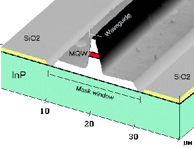
Fig. 5 Atomic force microscopy picture of the waveguide sample grown on a patterned (100) InP substrate, sample 389. The waveguide was processed in the center of the 20 µm window which is surrounded by 45 µm wide mask lines.
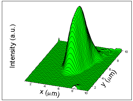
Fig. 6 Near-field image of the beam guided along the waveguide sample grown on a patterned (100) InP substrate, sample 389. The waveguide was processed in the center of the 20 µm window which is surrounded by 45 µm wide mask lines.
The results obtained can be found in the following references:
Influence of mask design on the selectivity mechanisms of InGaAs/InAlAs quantum wells grown on patterned substrates
F. Racedo, M. P. Pires, B. Yavich, L. C. D. Gonçalves e P. L. Souza
Materials Science and Engineering B: Solid-State Materials For Advanced Technology 74, 12, 2000.
Influence of mask design on the optical transition energy of InGaAs/InAlAs quantum wells grown by selective area epitaxy
B. Yavich, F. Racedo, M. P. Pires, L. C. D. Gonçalves e P. L. Souza
Proceedings da 8th European Workshop on Metalorganic Vapor Phase Epitaxy, Praga, República Tcheca, june 1999.
Influence of mask design on the selectivity mechanisms of InGaAs/InAlAs quantum wells grown on patterned substrates.
F. Racedo, M. P. Pires, B. Yavich, L. C. D. Gonçalves e P. L. Souza
Proceedings da 3rd International Conference on Low Dimensional Structures and Devices, Antalya, Turquia, september de 1999.