Structures with planar doping
:: References :: Other projects
Planar or delta doping consists in introducing a doping plane in a material. Delta doping can lead to higher mobilities since the carriers are, in the average, more distant from the ionized impurities than in the case of conventional homogeneous doping. A plane of impurities introduces a V-shaped potential for n-type doping and an inverted V-shaped potential for p-type doping. It is also possible to obtain a doping superlattice, that is, several doping planes separated by a fixed distance.
n-type delta doping in InP, where the dopant is Si, has been studied in great detail. An impurity localization below 8 Å has been achieved. The impurity localization has been determined by CV profiling together with a self-consistent calculation of the Schrödinger and Poisson equations. Delta doping superlattices with periods varying from 100 to 250 Å have also been obtained. Photoluminescence spectra of such structures revealed a cut-off energy which depends on the period. In addition, a 2D to 3D transition has been observed when the period is reduced. Transport measurements allowed for a detailed evaluation of the carriers distribution among the different subbands or minibands and of their mobilities.
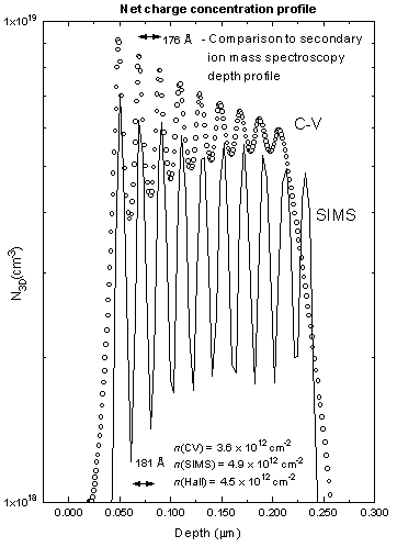
Fig. 1 Depth profile for sample 200 of the net charge concentration measured by C-V (scattered plot) and the Si atomic concentration measured by SIMS (solid line plot).
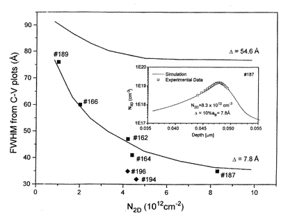
Fig. 2 Full width at half maximum (FWHM) of the C-V plots as a function of the carrier sheet concentration. The squares represent the experimental points for the single delta-doped layers while the diamonds correspond to the periodical structures. The lower and upper solid lines are the result of a numerical simulation assuming an impurity spread over 10 % and 70 % of the Bohr radius, respectively. The insert shows the net charge concentration as a function of depth for the single delta doped InP sample #187. The squares are the experimental points obtained from a C-V depletion profile while the solid line is a simulation assuming an impurity distribution over 10 % of the Bohr radius (aB). Included in the figure is the carrier sheet concentration obtained from Hall measurements.
InP barriers with thickness varying from 30 to 150 Å, imersed between two InGaAs layers, containing a n-type doping plane in the center were grown. The electronic structure which optimizes the conductivity can be obtained by investigating such barriers between the limits of zero thickness (InGaAs containing a doping plane) and infinite thickness (InP with a doping plane). The thickness of the InGaAs and InP layers and the structural properties of the InGaAs/InP interfaces were evaluated using X-ray diffraction and photoluminescence. In addition, the carrier concentration and the mobility were measured by Hall effect, Shubnikov-de Haas and also by photoluminescence at low temperatures together with a self-consistent calculation.
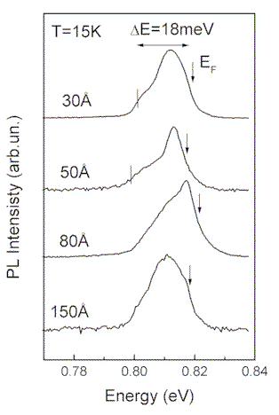
Fig. 3 Photoluminescence spectra for the samples with delta doped barriers. The Fermi level is approximately at 820±2 meV for all samples and coincides with the value associated to the alloy composition determined from the X-ray spectra. The total carrier density was estimated from the value of DE.
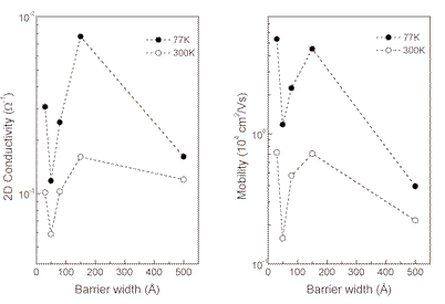
Fig. 4 Mobility and conductivity as a function of barrier thickness. The solid lines are a guide for the eyes. The data for the sample with 500 Å barrier correspond to an interpolation of the data for InP bulk samples with a doping plane.
InGaAs/InP MQW with n-delta doping in the barriers were also studied. The investigated samples contained QW with a fixed thickness of 50 Å and barriers with thicknesses varying from 20 to 50 Å. Photoluminescence spectra revealed the presence of a two dimensional electron gas. X-ray diffraction allowed the determination of the period of the superlattice, the QW alloy composition and the quality of the InGaAs/InP interfaces. Shubnikov-de Haas measurements together with a self-consistent calculation of the electronic structure indicate that a Si segregation in the growth direction may occur. A reduction in the carrier concentration with the decrease in the barrier thickness reveals that the interface plays a role in the carrier trapping. Such a reduction in the carrier concentration is also observed with photoluminescence under magnetic field.
Finally, GaAs/AlGaAs superlattices with n-type delta doping in the QW and p-type delta doping in the barrier were grown. Carbon is used as the p-dopant. The introduction of planar nipi doping superlattice in the MQW structure should increase the Stark shift, and therefore, such MQW structure should be a more appropriate for amplitude modulators based on the Stark effect.
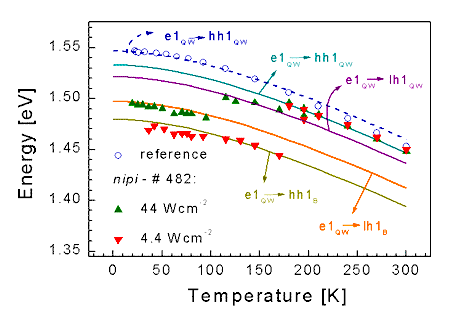
Fig. 5 Luminescense peak energy as a function of temperature. It can be observed that at low temperatures the transition energy is smaller than that of an undoped sample. For higher temperatures the optical transition energy follows that one of an undoped sample. A change from indirect (e1QW - hh1B) to direct (e1QW - hh1QW)transition takes place, as the curves (solid lines) calculated using the k·p model show.
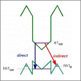
Fig. 6 Energy band showing the direct and indirect transitions in a quantum well structure with an nipi delta-doped superlattice.
The results obtained can be found in the following references:
nipi delta-doping superlattices for amplitude modulation
C.V.-B. Tribuzy, S. M. Landi, M. P. Pires, R. Butendeich, P. L. Souza, A. C. Bittencourt, G. E. Marques e A. B. Henriques
Brazilian Journal of Physics 32, 269 a 274 (2002).
Investigation of the interfaces and dopant incorporation in InP/InGaAs superlattices
L. Hanamoto, C. V.-B. Tribuzy, A. B. Henriques, P. L. Souza e B. Yavich
Brazilian Journal of Physics 32, 334-337 (2002).
Delta-doping Superlattices in Multiple Quantum Wells
Christiana V.-B. Tribuzy, Maurício P. Pires, Rainer Butendeich, Sandra M. Landi, Patrícia L. Souza, Gilmar E. Marques, A. C. Bittencourt e André Henriques
Physica E 11, 261-267 (2001).
Carbon delta-doped AlGaAs
Christiana V.-B. Tribuzy, Rainer Butendeich, Maurício P. Pires, Patrícia L. Souza e André Henriques
Journal of Applied Physics 90, 1660 (2001).
Electronic scattering in doped finite superlattices
A. B. Henriques, P. L. Souza e B. Yavich
Physical Review B 64, 45319 (2001).
Anisotropy of the cyclotron mass in superlattices containing two populated minibands
A. B. Henriques, P. L. Souza e B. Yavich
Semiconductor Science and Technology 16, 1 (2001).
Magneto-photoluminescence of Tamm states in InP/In0.53Ga0.47As superlattices
A.B. Henriques, R.F. Oliveira, P.L. Souza and B. Yavich
Physica B 298, 320 (2001).
Observation of densely populated Tamm states in modulation doped superlattices
A. B. Henriques, L. K. Hanamoto, P. L. Souza e B. Yavich
Physical Review B 61, 13369, 2000.
Delta- Doping in InP and Related Compounds
P. L. Souza
Capítulo no livro InP and Related Compounds editado por Omar Manasreh, Gordon and Breach Science Publishers SA, USA, 2000.
Si segregation and interface quality in InP/InGaAs superlattices assessed by magnetotransport measurements
A. Henriques, L. Hanamoto, P. L. Souza, L. C. D. Gonçalves e B. Yavich
Apresentação na 20th International Conference on Defects in Semiconductors em Berkeley, CA, USA, julho de 1999.
Properties of InP delta-doped barriers in InGaAs alloys
L. C. D. Gonçalves, B. Yavich, P. L. Souza e A. Henriques
Apresentação no 9th Brazilian Workshop on Semiconductor Physics, Belo Horizonte, MG, Brasil, fevereiro de 1999 e artigo em elaboração.
High Magnetic field transport and luminescence in doped InGaAs/InP superlattices
A.B.Henriques , L.K.Hanamoto , P.L.Souza , L.C.D.Gonçalves e B.Yavich
Apresentação no 9th Brazilian Workshop on Semiconductor Physics, Belo Horizonte, MG, Brasil, fevereiro de 1999.
Magnetic field induced Bragg reflections in artificially layered structures
André Henriques, P. Koenraad, L. C. D. Gonçalves, B. Yavich e P. L. Souza
Proceedings da 24th International Conference on the Physics of Semiconductors, Jerusalem, Israel, World Scientific (1998).
Si delta-doping superlattices in InP grown by LP-MOVPE
P. L. Souza, B. Yavich, M. Pamplona-Pires, A. B. Henriques e L. C. D. Gonçalves
Radiation Effects and Defects in Solids 146, 81, 1998 e apresentação no Symposium on Defect Dependent Processes in Insulators and Semiconductors, Campos do Jordão, Brasil, julho de 1997.
Electronic and Optical Properties of Periodically Si delta-Doped InP Grown by Low Pressure Metalorganic Vapor Phase Epitaxy
P. L. Souza, B. Yavich, M. Pamplona-Pires, A. B. Henriques e L. C. D. Gonçalves.
Journal of Applied Physics 82, 700, 1997.
Ionized Impurity scattering in periodically delta-doped InP.
A. B. Henriques, L. C. D. Gonçalves, N. F. Oliveira Jr., P. L. Souza e B. Yavich
Physical Review B 55, 13072, 1997.
Quantum transport in periodically delta-doped GaAs
L. C. D. Gonçalves, A. B. Henriques, N. F. Oliveira Jr., S. M. Shibli, P. L. Souza e B. Yavich
Zeitschrift für Physik B 104, 457, 1997.
Single and Periodically Si delta-doped InP grown by LP-MOVPE
B. Yavich, P. L. Souza, M. Pamplona Pires, W. M. Mendes, A. B. Henriques, e L. C. D. Gonçalves
Semiconductor Science and Technology 12, 481, 1997 e apresentação como Late News na 8th International Conference on MOVPE Growth Cardiff, Inglaterra, junho de 1996.
Band Gap Renormalization in Periodically Delta-Doped Semiconductors
A. B. Henriques, S. Obukhov, L. C. D. Gonçalves, P. L. Souza e B. Yavich
Physica Status Solidi 164, 133, 1997.
Characterization of periodically delta-doped semiconductors by capacitance-voltage profiling
L. C. D. Gonçalves, A. B. Henriques, P. L. Souza e B. Yavich
Semicond. Sci. and Technol. 12, 1, 1997.
Magnetic quantum effects in periodically delta-doped semiconductors
A. B. Henriques, L. C. D. Gonçalves, P. L. Souza e B. Yavich
Brazilian Journal of Physics 27, 38, 1997.
Photoluminescence and Mobility of Single and Periodically Si-Delta-Doped InP Grown by LP-MOVPE
B.Yavich, P. L. Souza, M. Pamplona Pires, A. B. Henriques e L. C. D.Gonçalves
Brazilian Journal of Physics 27, 189, 1997 e apresentação no 8th Brazilian Workshop on Semiconductor Physics, Águas de Lindóia, SP, Brasil, fevereiro de 1997.
Capacitance-voltage profiling of prtiodically delta-doped semiconductors
A. B. Henriques, L. C. D. Gonçalves, P. L. Souza e B. Yavich
Brazilian Journal of Physics 27, 215, 1997 e apresentação no 8th Brazilian Workshop on Semiconductor Physics, Águas de Lindóia, SP, Brasil, fevereiro de 1997.
Sample parameters of degenerate semiconductor superlattices
L. C. D. Gonçalves, A. B. Henriques, P. L. Souza e B. Yavich
Brazilian Journal of Physics 26, 327, 1996 e apresentação no 7th Brazilian Workshop on Semiconductor Physics, Rio de Janeiro, RJ, Brasil, julho de 1995.
Characterization of delta-doped superlattices by Shubnikov-de-Haas
A. B. Henriques, L. C. D. Gonçalves, P. L. Souza e B. Yavich
Semicond. Science and Technol. 11, 190, 1996.
Photoluminescence of periodically delta-doped InP
A. B. Henriques, L. C. D. Gonçalves, P. L. Souza e B. Yavich
Proceedings da 12th International Conference on Application of High Magnetic Fields in Semiconductor Physics, editado por Landwehr e Ossau, vol. 2, 629, Würzburg, Alemanha, World Scientific (1996).
Multisubband scattering in periodically delta-doped InP
A. B. Henriques, L. C. D. Gonçalves, P. L. Souza e B. Yavich
Proceedings da 23rd International Conference on the Physics of Semiconductors, 2363, editado por M. Scheffler, Berlim, Alemanha, World Scientific (1996).
Magnetic breakdown in delta-doped GaAs superlattices
A. B. Henriques, V. N. Morgoon, P. L. Souza, V. Bindilatti, N. F. de Oliveira e S. M. Shibli
Phys. Rev. B 49, 11248, 1994.